Pages

Tuesday, June 28, 2011

Control system(INPUT- OUTPUT RElATION

                Introduction & Background
 >>Control system is the behavior of the system is    described by the differential equations. The differential equation may be ordinary differential equation or difference equation.
  
 >>The first significant control device was James Watt's fly-ball governor. It was invented in 1767. the working principle was to keep the speed of the engine constant by regulating the supply of the steam to the engine.
           
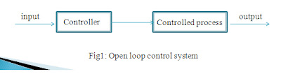
             What is open loop control system?

 
The control system  without feedback is called open loop control
system or non feedback control system. In open loop systems the
control action is independent on the desired output.
Examples: Automatic washing machine, Immersion rod, a field control D.C motor.

 Advantages of open loop control system
  • Open loop control system are simple.
  •  Open loop control system are economical.
  •  Less maintenance is required and not difficult.
  •  Proper calibration is not a problem.
     Disadvantages of open loop control system
  •  Open loop control system are inaccurate.
  •   These are not reliable.
  •   These are slow.
  •  Optimization is not possible     
       What is close loop control system? 
 Close loop control systems are known as feedback control system.
In close loop control system the control action is dependent on the
desired output. 
Example: Air conditioners provided with thermostat. 


 Advantages:  

  • These systems are more reliable.
  •   Close loop systems are faster.
  •  A number of variable can be handled simultaneously. Optimization is possible 


      Disadvantages :
  •  Close loop systems are expensive.
  •  Maintenance is difficult.
  •  Complicated installation 
                     What is transfer function?
Transfer function is defined as the ratio of Laplace transform of the
output to the Laplace  transform of input with all initial conditions
are zero.
Consider a open loop control system                                
   R(s) = Laplace  transform of input.             
   C(s)= Laplace transform of output.
   G(s)= Transfer function.
 
Transfer function G(s)=C(S)/R(S)


 Characteristics equation of a transfer function

Characteristics equation of a transfer function is 

 
POLES:  The poles of G(s) are Those values of ‘s’ which make G(s)
tend to infinity. Above transfer function having simple poles at
 s=0,s=-2,double poles at s= -4
ZEROS:The zeros of G(s) are Those values of ‘s’ which make G(s)
tend to Zero. Here the simple Zero at s= -3.
Graphical representation of POLES & ZEROS 
Poles are represented by ‘X’ & Zeros are represented by ‘O’.
Now the Pole-Zero plot of the previous transfer function is
 

           Time Response of Control system
Time domain representation of a control system is known as time
response . Time response of a control system is divided into two
parts. 
  1. Transient response        
   2.  Steady state response        
Time response of the 1st order system with unit step input 


 Some definitions of transient response of 2nd                                order system
 DELAY TIME: It is the time required for the response to reach 50% of  the final value in first time.
RISE TIME: It is the time required for the response to rise 10% to 90% of its final value for over-damped system and 0 to 100% for under damped system 
 PEAK TIME: It is the time required for the response to reach the first peak of the time response or first peak overshoot
MAXIMUM OVERSHOOT: It is the normalized difference between the peak of the time response and steady output.
 
SETTLING TIME: It is the time required for the response to reach and stay within the specified range   (2% to 5%) of the final value.
 
STEADY STATE ERROR:  It is the difference between actual
 output and desired output as time ‘t’ tends to infinity.


Monday, June 27, 2011

Transistor

TRANSISTOR:
A transistor has three-layer semiconductor device consisting of either two n- and one p-type layers of material or two p- and one n-type layers of material. The former is called an npn transistor, while the called an pnp transistor.             
There are two kinds of transistor.  
1.  P-N-P transistor  
2.  N-P-N transistor 
Working of N-P-N transistor:
The n-p-n transistor with forward bias to emitter bias junction and reverse bias to collector-bias junction. The forward bias causes the electron in the n-type emitter to flow towards the base. This constitutes the emitter current IE .  As these  electrons flow through the P-type base, they tend to combine with hole. As the base is lightly doped and very thin, therefore, only a few electrons combine with holes to constitute base current IB . In this way entire emitter current flows in the collector circuit. The emitter current is the sum  of collector and base current I, e. IE = IB + IC Working of P-N-P transistor:

The basic connection of  p-n-p transistor. The forward bias causes the electron in the p-type emitter to flow towards the base. This constitutes the emitter current IE .  As these holes cross into n-type base, they tend to combine with electrons. As the base is lightly doped and very thin, therefore, only a few holes combine with electrons to constitute collector region to collector current IC . In this way entire emitter current flows in the collector circuit. The emitter current is the sum  of collector and base current  .
 

Bipolar Junction Transistor: 
A bipolar junction transistor (BJT) is widely used in discrete circuits as well as in IC design, both analog and digital.  Its main applications are in amplification of small signals, and in switching digital logic signals.  In a BJT, both majority carriers and minority carriers play a role in the operation of the transistor, hence the term bipolar.


Sunday, June 26, 2011

DIGITAL CLOCK PROJECT REPORT


Introduction:
                                We know that 60 seconds equal to 1 minute and 60 minutes equal to 1 hour. Hence the minute section is drived by second section and hour section by the minute section. Each of the minute and second section has been designed to give a count from 00 to 59 after which it resets to 00. and the hour section to give a count from 00 to 11 hours after which it resets to 00. For each cycle of 00 to 59 in second section the minute section increases its count by 1. Similarly for each cycle of 00 to 59 in minute section the hour section increases it’s count by 1. In this way when the clock reaches 11hrs. 59mins. 59secs. each of the section resets to 00 giving us a display 00.00.00  popularly known as the 0th hour.            
                                              *                                                                     *   
                                 Now,  without  wasting  any  time  we  straightaway  move  into  the discussion with our project with emphasis on different sections considering the modules.

Module Structure:

                     The entire project has been divided into four modules. They are as follows:
  •   Second section
  • Using two counter ICs (IC 7490) in such a way that this portion produces output from 00 to 59 continuously with a frequency of 1 z (1pps).
  •   Using Driver IC (IC 7447) and seven-segment  display the counts. Both the ICs are of common anode type.
  •    Checking the output of the circuit.

  •  Minute section
Ø  Repeating the same circuit as that of the second section, but here the output should count from 00 to 59 with a frequency of 1Hz.for 1 ppm.
Ø  Checking the output.  

  • Hour section
Ø   Designing the circuit in such a way so that the output resets to 00 automatically displaying 11.59.59
Ø   Here the counting proceeds with a frequency of one pulse per hour.
Ø  Checking the output. 

Ø  Assembling the three sections together.
Ø Checking the output the final circuit.

 Block Diagram


Basic Concept
                             It is evident from the block diagram that for each of Second and
Minute section we require a Counter for the unit’s place and  ten’s place. For the second and minute sections the situation is identical with the unit’s place counting from 0-9-0 and repeats whereas the ten’s place counts from 0-5-0 and repeats. For the Hour section we require the counter for the unit’s place to count 0-2-0 and for the ten’s place it counts 0-1-0 and repeats. The circuit could have been easily designed with an IC 7476 i.e. a dual J-K Flip-Flop but to maintain parity between the components used we stick to the basics by using IC- 7490 (details mentioned later). 

Components used
                              
                                                 Material                                      Quantity  
                                                    IC 555                                    ----- 1(for all section)
                                                    Ic 7408                                   -----2
                                                    IC 7490 (14 pins)                   -----  6 (2 for each section)
                                                    IC 7447 (16 pins)                   -----  6 (2 for each section)
                                                    7 -segment display                  -----  6(2 for each section)
                                                    Resistances 1kΩ                     -----  7 (all total)
                                                    Resistances 2.2MΩ                ---- -  1
                                                   Capacitor 0.1F+1F     -----  1+1
Component Description
     IC 7490
   
                                               
                                                 The IC 7490 is a 4-bit, ripple-type Decade counter. The device consists

of four master-slave flip-flops internally connected to provide a divide-by-two section and a divide-by-five section. Each section has a separate clock input to initiate state changes of the counter on the High–to-Low clock transition. State changes of the Q outputs do not occur simultaneously because  of internal ripple delays. Therefore decoded output signals are subject to decoding spikes and should not be used for clocks or strobes.

                                      A gated AND asynchronous Master Reset (MR1 – MR2) is provided which overrides both clocks and resets (clears) all the flip-flops. Also provided is a
gated AND asynchronous Master Set (MS1-MS2), which overrides the clock and the
MR inputs , setting the output to nine (HLLH).       
N.B.: In the fig. Master Reset and Master Set have been denoted by R1, R2 & S2, S2  respectively.

IC 7447   & Seven-segment Display


                          Fig:c                                    Fig:d        

According to the Pin configuration
                   LT=Lamp Test  >>After doing every connection between the chip and the segment if  this terminal (LT) is grounded then all segment will glow. In the working mode LT
should always be High.
BI/RBO=Blanking input/Ripple blanking Output >> when this terminal is grounded the display will be blank immediately.
RBI=Ripple Blanking input. When this terminal is grounded and the input code is set
for zero display then the display will be blank immediately and zero will come out independent of LT.
In the IC a, b, c, d, e, f, g are the pins which are connected to the seven-segment
display and the parts which blink for these connections are shown above.   

MODULE Details 

Seconds Section:
                           
                        Since the basic concept regarding the counting of the seconds has been discussed we are now going to design the circuit. Since the count is from 00-59 we would design a MOD-60 counter by cascading a MOD-10/ Decade Counter and a MOD-6 Counter. The IC-7490 is a Decade Counter with two parts (internal structure): MOD-2 and MOD-5 Counter. So we would design the MOD-6 counter basically from a Decade Counter.
                         Using the reset pins as shown in Fig.2a we can design any MOD-K Counter by the internal components --Mod-2 and Mod-5 counters of a particular IC-7490. 
                        A Clock of 1 Hz. Frequency is supplied to the unit’s part of the second’s section at a rate of 1 pulse per  second (1pps). On the other hand the ten’s part is getting anegative-edge trigger which is the clock for the ten’s part. The clock pulse is applied from Q3 .The reason being  it resets after nine represented in binary as:

                                                             Q3    Q2    Q1    Q0 
                                                        9=    1      0      0       1
                     The output of this part is solely responsible for driving the minute section i.e. acting as a clock for the minute section. From the truth table (Table 1.) we see for MR1 &
MR2 both equal to 1 the clock is reset and the output is zero.
  In the ten’s part the count resets to 0 after 5.       
                                                                              Q3    Q2    Q1    Q0 
Representing ‘6’ in binary form we have               6 =0       1      1       0 
 Taking the high inputs Q2 Q1 we apply to the reset pins to solve our purpose.

Circuit Diagram


                                The Circuit that has been exactly designed is shown here.


Minute Section

                             The Minute section is nothing but  an exact replica of the second’s section as the theory and implementation is the same with one major exception i.e. the clock from the second’s section is applied to the unit’s place of the minute’s section at a rate of 1 pulse per minute (1ppm). 

Hour Section


                           For the Hour section we have an  altogether a different circuit design
where the unit’s place counts from 0-9 one and 0-1 once in this sequence. Here the
counting takes place from 00- 11 and resets back to 00. For the unit’s place we use a
Decade counter as done previously. And for the ten’s place we have designed a
MOD-3 counter simply using the MOD-5 counter part of IC-7490. We, now, check
the condition for which the hour section should reset.
                                             Tens             Units
                for                         0                     4  
                or                          1                     0                           the clock is not reset to ‘0’
            But for                      1                     1                            the clock is reset to ‘0’ 

Thus if the two reset pins of the two counters are connected with each other (i.e. MR1
& MR2 ) and MR1  is again connected with Q2 of the unit’s place and MR2 is
connected with Q1 of the ten’s place then the clock is reset after 11 to 00.        
                                                                                          Q3    Q2      Q1    Q0
 Since binary representation of,                                     1=    0       0        0         1
                                                                                   2=    0       0        1         0

Thus Q1 of the ten’s place and Q2 of the unit’s place reset each other. Since
MR1 =Q2 of the unit’s place=1 and MR2 =Q1 of the ten’s place =1. Since both MR1 &
MR2 are high they need to reset the clock to 0 after 11.59.59 to 00.00.00, which is
known as the 0th hour.
For the hour section the clock drives it’s unit’s place from Q2 of the ten’s place of the minute section and the clock pulse is produced at the rate of 1 pulse per hour,i.e.1pph.
In the following page we have the circuit for the hour section with the internal circuitry connections shown. 
 
Circuit Diagram
 
Assembling the three sections

                              Now that the circuit designing part is more or less complete the hard
work is over and we assemble the three sections (seconds, minute and hour) to get the 
“Digital Clock”. With the supply connected we operate the clock to check the output.
The clock was found to operate smoothly.


Conclusion

                            The Circuit was  purely  designed with  the  basic  knowledge  on  sequential
circuit designing and with the components  provided by the authority. The Clock is
expected to operate normally with desired accuracy.